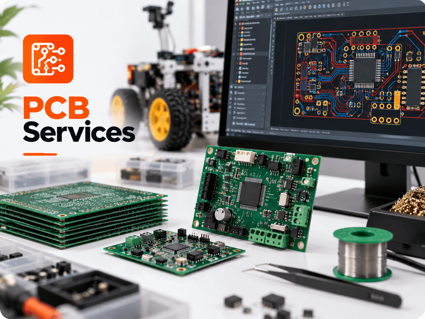
In electronics engineering, the terms 'PCB' and 'PCBA' are often used interchangeably by beginners, but they refer to two completely different manufacturing stages. A bare Printed Circuit Board (PCB) is simply an unpopulated green (or black/blue) fiberglass board with etched copper tracks and plated holes. In contrast, a Printed Circuit Board Assembly (PCBA) is a completed, fully functional electronic circuit populated with microcontrollers, resistors, capacitors, and connectors soldered into place. Understanding this distinction is essential when requesting quotes and planning hardware timelines.
Phase 1: Bare Board PCB Fabrication
Fabrication is a chemical and mechanical manufacturing process that creates the bare substrate:
- 1Substrate Lamination: Using FR-4 glass-reinforced epoxy clad with copper foil.
- 2Photolithography & Etching: Applying photoresist, exposing the circuit pattern to UV light, and chemically dissolving unwanted copper to form electrical traces.
- 3Drilling & Plating: Drilling via holes and component holes, then electroplating copper inside the hole barrels to connect layers.
- 4Solder Mask Application: Coating the board with protective polymer resin (green, matte black, etc.) leaving only pads exposed for soldering.
- 5Surface Finishing: Applying Lead-Free HASL or ENIG (gold) to prevent exposed copper oxidation.
- 6Silkscreen Legend: Printing component designations and logos.
- 7Electrical Testing: Running automated Flying Probe continuity tests to ensure zero opens or shorts.
Phase 2: PCB Assembly (PCBA)
Once bare boards are fabricated, assembly transforms them into functional hardware:
- 1Solder Paste Stenciling: A precision stainless-steel laser-cut stencil deposits solder paste onto SMD pads.
- 2Automated Pick-and-Place: High-speed SMT placement heads position microscopic surface-mount components according to the centroid coordinate file.
- 3Reflow Soldering: The board passes through a multi-zone reflow oven with controlled thermal ramp-up, melting solder paste to form metallurgical joints.
- 4Through-Hole (THT) Insertion: Connectors, large electrolytic capacitors, and relays are manually or wave-soldered.
- 5Bench Inspection & Bring-Up: Technicians inspect joints under high-magnification microscopes and verify DC power rails before dispatch.
| Parameter | Bare PCB Fabrication | Turnkey PCBA Assembly |
|---|---|---|
| Deliverable | Unpopulated circuit board | Populated, operational electronics board |
| Files Needed | Gerber files + Drill files | Gerbers + BOM with MPNs + Centroid (Pick & Place) |
| Primary Materials | FR-4 laminate, copper foil, solder mask ink | Bare PCB + SMD/THT components + solder paste |
| End State | Passive mechanical substrate | Active computing/control hardware |
Order Turnkey Bare Boards or Full PCBA →
Go Now