
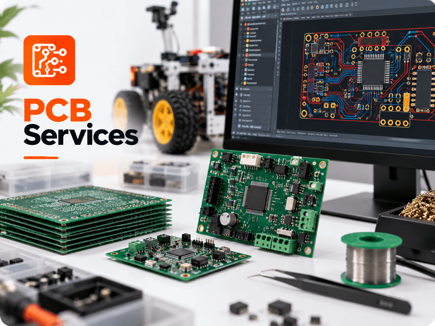
Understanding the distinction between PCB Design, PCB Fabrication, and PCB Assembly (PCBA) is essential for engineers, hardware startups, and purchasing managers bringing electronic products to market.
Stage 1: PCB Design & Gerber Preparation
PCB design is the software engineering phase where circuit schematics are translated into physical copper trace geometry. Designers perform trace routing, power plane decoupling, and Design Rule Checks (DRC) before exporting industry-standard Gerber RS-274X files and NC drill data.
Stage 2: Bare Board PCB Fabrication
PCB fabrication is the chemical and mechanical manufacturing process that creates the bare printed circuit board. FR-4 glass epoxy laminates undergo copper etching, multi-layer lamination, drilling, electroplating, solder mask application, and surface finishing (HASL or ENIG).
Stage 3: Printed Circuit Board Assembly (PCBA)
PCB assembly mounts electronic components onto the bare fabricated board. Surface-mount technology (SMT) pick-and-place machines position fine-pitch ICs onto solder paste, followed by reflow oven curing and automated optical inspection (AOI).
| Phase | Primary Input | Output Deliverable | Key Quality Indicator |
|---|---|---|---|
| 1. Design | Circuit Schematic & Component Specs | Gerber RS-274X & BOM Files | Zero DRC / DFM Violations |
| 2. Fabrication | Gerber & NC Drill Files | Bare FR-4 Printed Circuit Board | Impedance accuracy & 100% E-test pass |
| 3. Assembly (PCBA) | Bare Board + Components + Stencil | Fully Assembled Functional PCBA | Zero solder bridges, cold joints or tombstoning |
Get Turnkey PCB Design, Fab & PCBA Quote →
Go Now