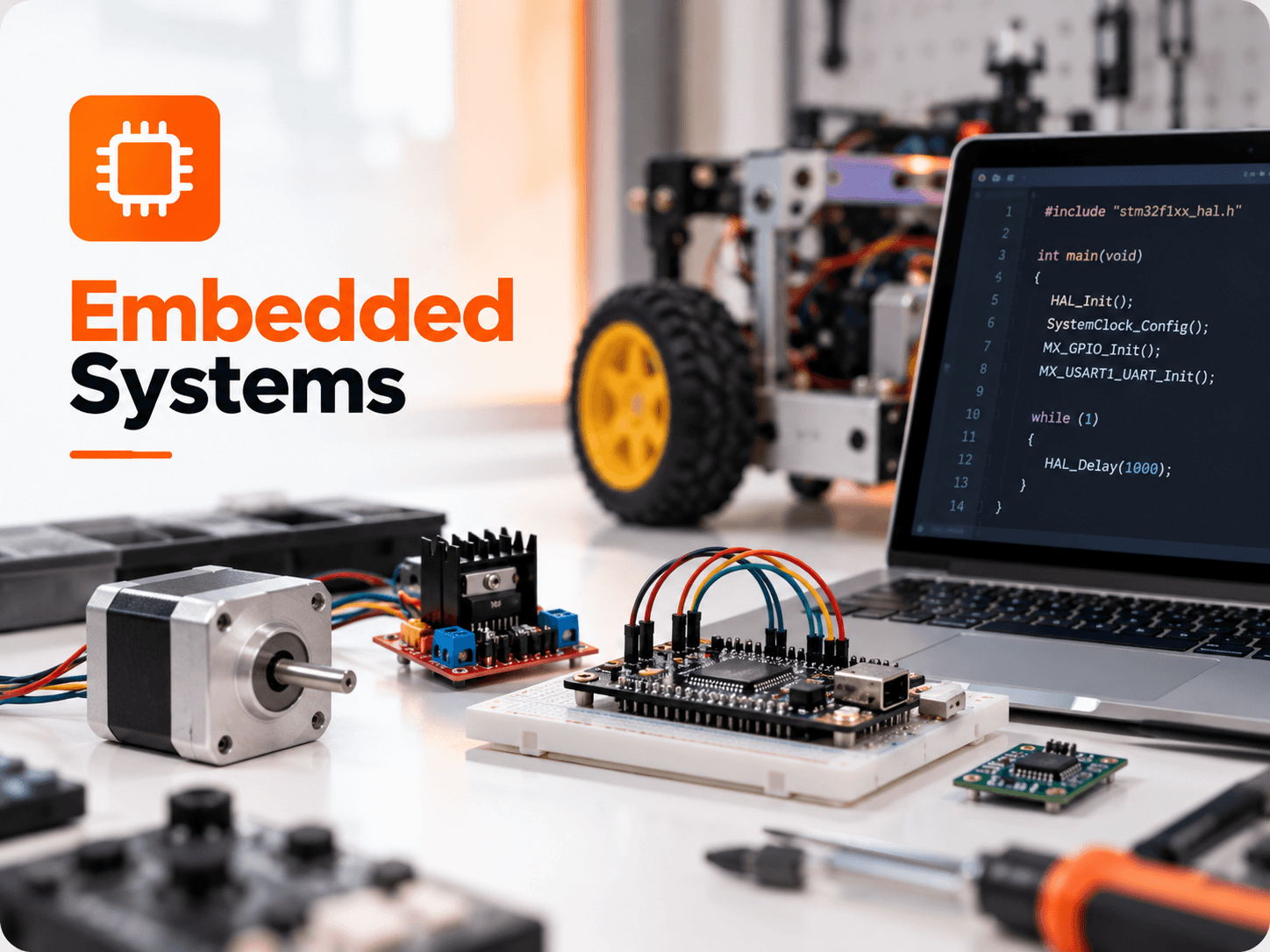
Building prototypes with off-the-shelf development boards (ESP32 DevKit, STM32 BluePill/Nucleo) is great for initial firmware proof-of-concept. However, commercializing an IoT sensor node, industrial controller, or autonomous robot requires integrating microcontrollers directly onto a custom printed circuit board. Eliminating jumper wires, loose breakout modules, and redundant USB chips makes hardware vastly more reliable, compact, and cost-effective. Here is how to design robust custom boards for ESP32 and STM32 architectures.
1. ESP32 Hardware Guidelines: RF Antenna and Power Delivery
When incorporating the ESP32-WROOM-32 or ESP32-S3 module, the onboard PCB meandered inverted-F antenna (MIFA) requires strict mechanical placement:
- Antenna Keep-Out Zone: Position the antenna section hanging over the edge of the PCB or over a dedicated cutout. Never route copper traces, ground planes, or place metal mounting screws beneath or adjacent to the antenna area across all board layers.
- Power Supply Sizing: The ESP32's Wi-Fi radio draws instantaneous peak current pulses of up to 500mA during RF transmission. Use an LDO regulator (or buck converter) rated for at least 800mA to 1A with a 10µF low-ESR ceramic capacitor placed directly at the 3V3 power input pin.
- Boot Strapping Pins: Ensure GPIO0 and GPIO2 have proper pull-up/pull-down resistor networks to allow automatic serial flashing via a CH340 or CP2102 USB-to-UART transceiver.
2. STM32 Hardware Guidelines: Crystal Oscillators and Decoupling
STM32 microcontrollers (ARM Cortex-M0/M3/M4/M7) offer exceptional real-time deterministic performance for robotics, motor control, and industrial telemetry:
- Crystal Oscillator Layout (HSE/LSE): The external 8MHz/16MHz crystal and its load capacitors (typically 12pF to 22pF) must be placed as close as possible to the OSC_IN and OSC_OUT pins. Surround the crystal circuit with a dedicated ground guard ring to prevent stray noise coupling.
- Bypass Capacitor Distribution: Every single VDD/VSS pin pair on an STM32 must have a 0.1µF (100nF) ceramic capacitor connected with the shortest possible trace length directly to the pin before connecting to the ground plane.
- SWD Programming Header: Include a compact 4-pin or 5-pin 2.54mm header exposing SWDIO, SWCLK, NRST, 3V3, and GND for flashing with standard ST-Link debuggers.
| Subsystem | ESP32 Design Rule | STM32 Design Rule |
|---|---|---|
| Operating Voltage | 3.0V – 3.6V (strict 3.3V nominal) | 2.0V – 3.6V (or 1.8V on low-power lines) |
| Programming Port | UART (TX/RX + EN/GPIO0 auto-reset) | SWD (SWDIO + SWCLK) / JTAG |
| Critical Keep-Out | Antenna overhang; zero copper under RF | Crystal traces; short isolated traces with guard ring |
| Decoupling Strategy | 10µF bulk + 0.1µF high-frequency ceramic | 0.1µF on every VDD pin + 4.7µF on VDD_A |
Build Your Custom ESP32 / STM32 Hardware with Us →
Go Now